Pad printing for electronics is a highly precise and versatile printing process used to transfer a 2D image onto a 3D electronic component. Often called tampography, this method excels at printing high-resolution graphics, logos, and functional markings onto irregular, curved, or textured surfaces, making it an indispensable technology for manufacturing everything from connectors and switches to medical devices and consumer electronics casings. Its unique ability to conform to complex shapes with exceptional accuracy and durability sets it apart from other marking methods.
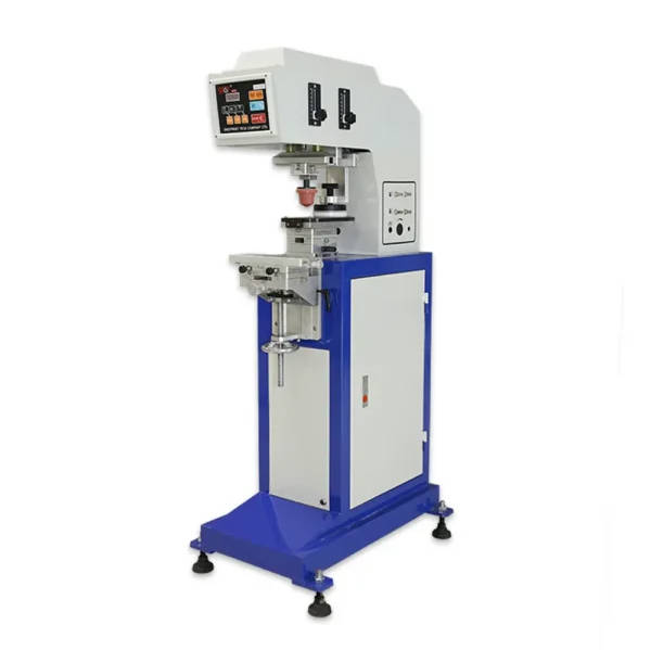
Table of Contents
- What is Pad Printing in the Electronics Industry?
- Why is Pad Printing the Preferred Method for Many Electronic Components?
- The Pad Printing Process: A Step-by-Step Breakdown for Electronics
- Mastering the Core Elements: A Deep Dive into Pads, Inks, and Clichés
- How to Achieve High Accuracy and Precision in Pad Printing
- Key Applications of Pad Printing in the Electronics Sector
- Pad Printing vs. Alternative Marking Technologies: A Comparative Analysis
- Overcoming Common Challenges in Pad Printing on Electronics
- The Future of Pad Printing in Electronics Manufacturing
- Conclusion: Why Pad Printing Remains a Cornerstone of Electronics Production
What is Pad Printing in the Electronics Industry?
At its core, pad printing is an indirect offset gravure printing process. This means that a silicone pad lifts a film of ink from an etched plate (known as a cliché) and transfers it onto the target object, or substrate. In the context of electronics, the substrate is typically a plastic casing, a metal connector, a ceramic-based component, or even a glass display. The magic of the process lies in the deformable nature of the silicone pad, which can wrap around curved surfaces, press into recessed areas, and conform to textured finishes, depositing a precise layer of ink every time.
This capability is what makes pad printing a go-to solution for the complex geometries found throughout the electronics industry. While a flat-bed printer struggles with anything but a perfectly flat surface, a pad printer can easily mark logos on contoured mouse casings, apply functional symbols to concave keyboard keys, print warning labels on cylindrical fuses, or place identifiers on multi-surfaced USB connectors. The process ensures that the printed image is crisp, complete, and undistorted, regardless of the part’s shape.
Why is Pad Printing the Preferred Method for Many Electronic Components?
The electronics industry relies on pad printing for a combination of reasons that other marking technologies cannot collectively match. The primary advantage is its unmatched versatility in printing on non-flat (3D) and irregular surfaces. From the subtle curve of a smart-watch bezel to the intricate topography of a multi-port hub, pad printing delivers where other methods fail. This makes it essential for both branding and functional marking on finished consumer products.
Furthermore, pad printing provides high-resolution and fine-detail printing. It can reproduce intricate logos, tiny alphanumeric codes for part traceability, and sharp, legible symbols on buttons and switches with remarkable clarity. The process is also highly adaptable to a wide variety of materials common in electronics, including ABS plastics, polycarbonate, nylon, glass, metals, and coated surfaces. By selecting the correct ink formulation, manufacturers can achieve excellent adhesion and durability, ensuring the markings withstand abrasion, chemicals, and environmental exposure throughout the product’s lifecycle.
The Pad Printing Process: A Step-by-Step Breakdown for Electronics
Understanding the mechanical sequence of pad printing demystifies how it achieves such precise results. While modern machines automate these steps at high speed, the fundamental process remains the same and can be broken down into five key stages.
Step 1: Artwork and Cliché (Printing Plate) Creation
Everything begins with the digital artwork. This design is then photochemically etched into the surface of a printing plate, or cliché. The cliché is a flat plate, typically made of hardened steel or a light-sensitive photopolymer, that contains a shallow, recessed version of the image to be printed. The depth of this etching is critical; it’s precisely controlled to hold a specific volume of ink, which directly influences the opacity and thickness of the final print on the electronic component.
Step 2: Inking and Doctoring the Cliché
The machine moves an ink cup (a sealed container with a sharp ceramic or metal ring) or a flood bar across the cliché, filling the etched image with ink. Immediately following this, a sharp, straight blade, known as a doctor blade, passes over the cliché’s surface. This action scrapes away all excess ink, leaving ink only within the recessed etching. The precision of this step is vital for a clean, sharp final image.
Step 3: Ink Pickup by the Silicone Pad
Next, the soft, pliable silicone pad is pressed down onto the etched, inked image on the cliché. The unique properties of silicone, combined with a slight solvent evaporation from the ink’s surface, cause the ink film to become tacky and lift cleanly out of the etching and onto the pad. The image now exists as a thin, wet film of ink on the surface of the pad.
Step 4: Transferring the Image to the Electronic Part
The machine then moves the pad over the electronic component, which is held securely in a custom fixture or jig. The pad descends and presses the ink-laden image onto the part. As the pad compresses, its flexible surface conforms perfectly to the shape of the component, whether it’s curved, angled, or textured. Upon lifting, the pad transfers nearly the entire ink film to the substrate, thanks to the ink’s greater affinity for the part’s surface than for the treated silicone pad.
Step 5: Curing the Ink for Permanent Adhesion
The final step is to ensure the ink permanently bonds to the electronic component. Depending on the ink system used, this involves either air drying, where solvents evaporate naturally; heat curing, where the part is passed through an oven to accelerate solvent evaporation and cross-linking; or UV curing, where the part is exposed to ultraviolet light to instantly polymerize the ink into a solid, durable state.
Mastering the Core Elements: A Deep Dive into Pads, Inks, and Clichés
The quality of a pad printed mark on an electronic device is not determined by the machine alone. It is the careful selection and interplay of three core elements: the pad, the ink, and the cliché. Mastering these components is the key to repeatable, high-quality results.
Choosing the Right Silicone Pad: Hardness, Shape, and Material
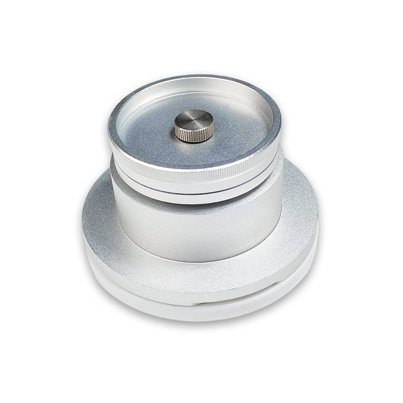
The silicone pad is the heart of the transfer process. Its selection is a science in itself. Hardness (Durometer) is the most critical factor. Pads come in various durometers, from very soft to very hard. A softer pad is excellent for heavily textured or curved surfaces as it can easily conform without applying excessive pressure, but it may have a shorter lifespan. A harder pad offers sharper image quality on flat or slightly curved surfaces and is more durable but may struggle to print a complete image on complex shapes. The shape of the pad—conical, rectangular, roof-shaped, or custom—is chosen based on the image size and the geometry of the part to ensure even pressure and a distortion-free transfer.
The Critical Role of Ink in Pad Printing for Electronics
The ink is arguably the most complex component. For electronics, inks must not only look good but also perform under demanding conditions. They must adhere strongly to various plastics (like ABS, PC, and PBT) and metals without causing damage. Key properties include abrasion resistance (for buttons and connectors), chemical resistance (to withstand cleaning agents), and electrical properties (specialty inks can be conductive or act as insulators). The choice of ink system—whether a one-component, two-component (epoxy-based), or UV-curable ink—depends entirely on the substrate, the required durability, and the production speed.
| Ink Type | Common Substrates | Curing Method | Key Properties | Typical Electronic Applications |
|---|---|---|---|---|
| 1-Component (Solvent-Based) | ABS, Polystyrene, PVC, Polycarbonate | Air or heat dry | Good adhesion, fast drying, easy to use | Logos on consumer electronics, markings on internal plastic components |
| 2-Component (Epoxy/Solvent-Based) | Metals, Glass, Thermoset Plastics, Powder Coats | Air or heat dry (catalyst-induced) | Exceptional durability, chemical & abrasion resistance | Medical devices, automotive electronics, military-grade connectors |
| UV-Curable | Most plastics, metals, glass | Instant UV light exposure | Extremely high durability, instant cure for high speed | High-volume production, keyboard keys, printed circuit boards (PCBs) |
| Specialty Inks | Varies | Varies | Conductive, dielectric, ceramic properties | Printed antennas, EMI/RFI shielding, markings on high-temp components |
Understanding Clichés (Printing Plates): Steel vs. Photopolymer
The cliché holds the master image and dictates the finest details possible. Photopolymer plates are flexible plastic plates that are cost-effective and easy to process in-house, making them ideal for short-to-medium production runs. They can resolve very fine details but have a limited lifespan (around 10,000-50,000 impressions). For high-volume electronics manufacturing, thick steel clichés are the standard. They are more expensive upfront but are incredibly durable, capable of lasting for over a million impressions while maintaining perfect image integrity. Their deeper and more consistent etch depth also allows for a more opaque ink deposit, which is often required for printing light colors on dark electronic casings.
How to Achieve High Accuracy and Precision in Pad Printing
In electronics, where components are shrinking and tolerances are tight, achieving repeatable accuracy is paramount. Several factors must be meticulously controlled to ensure every print lands in the exact same spot with perfect clarity.
The Impact of Machine Quality and Automation
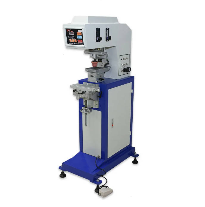
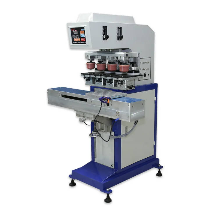
The foundation of precision is a high-quality, rigid pad printing machine. A robust machine minimizes vibration and deflection during the printing cycle, ensuring the pad and fixture maintain their precise X-Y-Z alignment. Modern machines often incorporate servo-electric controls instead of pneumatics for smoother, more programmable, and highly repeatable motion. Integrating vision systems for automatic part alignment and post-print inspection further elevates accuracy, automatically rejecting parts that do not meet strict quality standards.
Fixturing and Jigs: The Unsung Heroes of Precision
You can have the best machine in the world, but without a good fixture, you will never achieve precision. A fixture (or jig) is a custom-made tool that holds the electronic component in a precise, repeatable position for every print cycle. A well-designed fixture will nest the part securely without damaging it, preventing any movement during ink transfer. For multi-color jobs, a highly accurate fixture that ensures perfect registration between colors is absolutely critical.
Environmental Controls: Managing Static, Dust, and Temperature
The electronics manufacturing environment is often a cleanroom, and for good reason. Dust and debris are the enemies of perfect printing, causing pinholes and blemishes in the final mark. Likewise, static electricity, common with plastic components, can attract dust and even cause the ink to “fuzz” or spray during transfer. Anti-static air blowers are often used to neutralize the part just before printing. Consistent temperature and humidity are also important, as they affect ink viscosity and solvent evaporation rates, which in turn impact print quality and consistency.
Key Applications of Pad Printing in the Electronics Sector
The use of pad printing is widespread across the electronics industry, serving both aesthetic and functional purposes. Common applications include:
- Branding and Logos: Applying company logos and product names to casings for laptops, smartphones, power banks, and computer mice.
- Functional Markings: Printing symbols (power, volume, USB, HDMI), port labels, and switch positions on bezels, keyboards, and control panels.
- Regulatory Information: Marking parts with CE, UL, FCC logos, and other compliance information.
- Component Identification: Printing part numbers, batch codes, and orientation markers on integrated circuits (ICs), capacitors, relays, and circuit breakers for traceability and assembly.
- Medical Electronics: High-durability, biocompatible inks are used to mark catheters, monitoring devices, and surgical tools.
- Specialty Applications: Using conductive inks to print simple circuits, antennas, or RFID components directly onto plastic parts.
Pad Printing vs. Alternative Marking Technologies: A Comparative Analysis
While powerful, pad printing is not the only option. Understanding its strengths and weaknesses compared to other technologies is key to making the right choice for a specific application.
| Technology | Best For (Surface) | Resolution | Durability | Key Advantage | Key Limitation |
|---|---|---|---|---|---|
| Pad Printing | Irregular, curved, textured, recessed | High | Very High (with 2-component/UV ink) | Versatility on 3D shapes | Slower for large, flat graphics |
| Screen Printing | Flat or cylindrical | Medium | High | Thick, opaque ink deposit | Poor on complex curves |
| Laser Marking | Most materials (flat or slight curve) | Very High | Permanent (etches the surface) | No consumables, extremely precise | Cannot add color, can damage some plastics |
| Digital Inkjet | Flat or slightly curved | Very High (full color) | Medium to High | Full-color images, variable data | Adhesion/durability can be an issue |
Pad Printing vs. Screen Printing
Screen printing excels at applying thick, opaque layers of ink to flat or simple cylindrical surfaces. It’s great for large, bold graphics but lacks the ability of pad printing to conform to complex shapes and recessed areas.
Pad Printing vs. Laser Marking
Laser marking offers unparalleled permanence and precision as it physically alters the surface of the material. It’s ideal for serialization and anti-counterfeiting marks. However, it cannot add color (it only changes the color of the substrate) and can be unsuitable for heat-sensitive electronic components. Pad printing offers a full spectrum of colors and is a non-destructive process.
Pad Printing vs. Digital Inkjet
Industrial inkjet is fantastic for creating full-color, photorealistic images and for jobs requiring variable data (like unique serial numbers on each part). However, it is generally limited to flat or slightly curved surfaces, and achieving the same level of adhesion and chemical resistance as two-component pad printing inks can be a significant challenge.
Overcoming Common Challenges in Pad Printing on Electronics
Even with a perfected process, operators can face issues. Poor ink adhesion is a common problem, often solved by pre-treating the substrate with flame, corona, or plasma to increase its surface energy, or by simply ensuring the part is perfectly clean. Image “spidering” or “fuzzing” is typically caused by static and can be mitigated with ionization blowers. Inconsistent print quality can often be traced back to fluctuating ambient temperature or ink that is improperly mixed or has begun to cure in the cup.
Another challenge is printing on soft-touch coatings, which are popular on premium electronics. These surfaces can be difficult for inks to adhere to. The solution lies in working with an ink manufacturer to find a specialized ink series designed specifically to bond with that particular coating. Careful testing and process control are always the keys to overcoming these hurdles.
The Future of Pad Printing in Electronics Manufacturing
Pad printing continues to evolve. The drive for efficiency is pushing greater automation and robotic integration, where robots load and unload parts from fixtures, minimizing human contact and improving consistency in cleanroom environments. We are also seeing advancements in ink chemistry, with more robust and eco-friendly UV-LED curable inks that consume less energy. The integration of vision systems for real-time quality control is becoming standard, ensuring 100% inspection at full production speed. While fully digital pad printing is still a niche technology, ongoing research aims to combine the flexibility of digital with the versatility of pad transfer, potentially revolutionizing short-run and custom printing.
Conclusion: Why Pad Printing Remains a Cornerstone of Electronics Production
In the fast-paced and dimensionally complex world of electronics manufacturing, pad printing holds a unique and vital position. Its unparalleled ability to deliver high-resolution, durable markings onto the irregular and three-dimensional surfaces of modern components is a capability that other printing methods cannot easily replicate. By carefully controlling the core process and mastering the interplay between the machine, pad, ink, and cliché, manufacturers can achieve exceptional accuracy and quality. Pad printing is not just a method for applying a logo; it is a critical enabling technology that provides functionality, ensures traceability, and enhances the value and usability of electronic devices we use every day.
pad printing for electronics, pad printing accuracy, pad printing ink, pad printing process guide, electronic component marking, what is pad printing, tampography electronics, pad printing vs laser marking, silicone pad for electronics, cliché printing plate, uv pad printing ink